| CPC G06T 7/001 (2013.01) [G06T 7/337 (2017.01); G06T 7/97 (2017.01); G06T 2207/30148 (2013.01)] | 10 Claims |
|
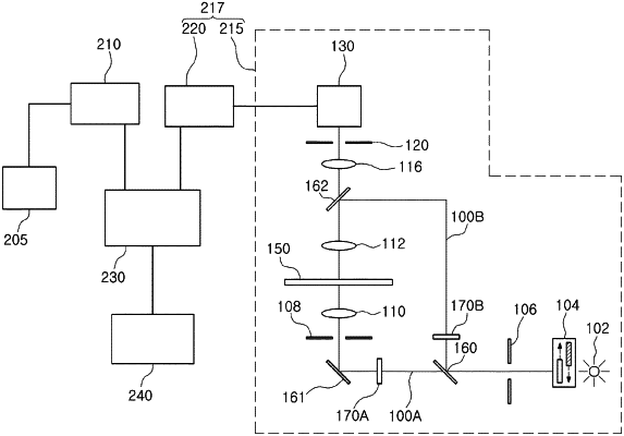
1. A method for inspecting a photomask in a defect inspecting apparatus, comprising:
generating a first reference image and a second reference image from design layout data of the photomask;
obtaining a first inspection image of a first inspection region of the photomask and obtaining a second inspection image of a second inspection region of the photomask by directing light onto the photomask;
extracting a first coordinate offset by comparing the first inspection image with the first reference image; and
extracting a second coordinate offset by comparing the second inspection image with the second reference image,
wherein the first reference image and the second reference image respectively include pixels smaller than pixels of the first inspection image and the second inspection image.
|