| CPC G06N 3/065 (2023.01) [G06N 3/082 (2013.01); G11C 7/1006 (2013.01); G11C 7/16 (2013.01); G11C 11/412 (2013.01); G11C 11/413 (2013.01); G11C 11/419 (2013.01); G11C 11/54 (2013.01); G11C 27/005 (2013.01); G06N 3/045 (2023.01); G11C 7/18 (2013.01); G11C 8/14 (2013.01)] | 10 Claims |
|
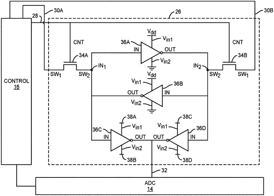
1. A static random-access memory (SRAM) system comprising a SRAM cell, the SRAM cell comprising:
a write word line;
a first write bit line and a second write bit line;
a read bit line;
a first read word line, a second read word line, a third read word line, and a fourth read word line;
a first inverter comprising an input coupled to a first intermediate node, an output coupled to a second intermediate node, a first voltage input node coupled to a supply voltage, and a second voltage input node coupled to a fixed voltage;
a second inverter comprising an input coupled to the second intermediate node, an output coupled to the first intermediate node, a first voltage input node coupled to the supply voltage, and a second voltage input node coupled to a fixed voltage;
a third inverter comprising an input coupled to the first intermediate node, an output coupled to the read bit line, a first voltage input node coupled to the first read word line, and a second voltage input node coupled to the second read word line;
a fourth inverter comprising an input coupled to the second intermediate node, an output coupled to the read bit line, a first voltage input node coupled to the third read word line, and a second voltage input node coupled to the fourth read word line;
a first switching element comprising a control node coupled to the write word line, a first switching node coupled to the first write bit line, and a second switching node coupled to the first intermediate node; and
a second switching element comprising a control node coupled to the write word line, a first switching node coupled to the second write bit line, and a second switching node coupled to the second intermediate node.
|