US 11,727,187 B2
Transmission gate manufacturing method
Shao-Lun Chien, Hsinchu (TW); Pin-Dai Sue, Hsinchu (TW); Li-Chun Tien, Hsinchu (TW); Ting-Wei Chiang, Hsinchu (TW); and Ting Yu Chen, Hsinchu (TW)
Assigned to TAIWAN SEMICONDUCTOR MANUFACTURING COMPANY, LTD., Hsinchu (TW)
Filed by TAIWAN SEMICONDUCTOR MANUFACTURING COMPANY, LTD., Hsinchu (TW)
Filed on Mar. 8, 2022, as Appl. No. 17/689,825.
Application 17/689,825 is a division of application No. 17/116,745, filed on Dec. 9, 2020, granted, now 11,295,055.
Application 17/116,745 is a continuation of application No. 16/530,703, filed on Aug. 2, 2019, granted, now 10,867,113, issued on Dec. 15, 2020.
Claims priority of provisional application 62/727,903, filed on Sep. 6, 2018.
Prior Publication US 2022/0188501 A1, Jun. 16, 2022
Int. Cl. G06F 30/398 (2020.01); G06F 30/392 (2020.01); G06F 30/394 (2020.01); G03F 1/36 (2012.01)
CPC G06F 30/398 (2020.01) [G03F 1/36 (2013.01); G06F 30/392 (2020.01); G06F 30/394 (2020.01)] 20 Claims
OG exemplary drawing
 
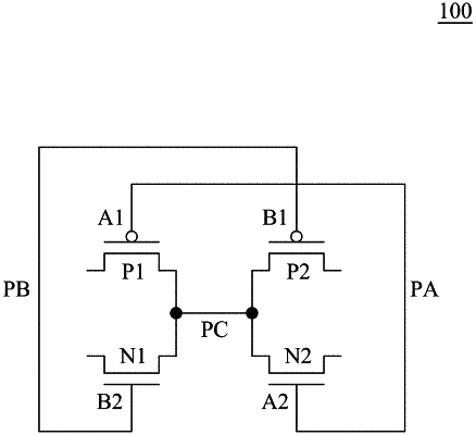
1. A method of manufacturing a transmission gate, the method comprising:
overlying a first active area with a first metal zero segment, the first active area comprising first and second PMOS transistors;
overlying a second active area with a second metal zero segment, the second active area comprising first and second NMOS transistors; and
configuring the first and second PMOS transistors and the first and second NMOS transistors as a transmission gate by forming three conductive paths, at least one of the conductive paths comprising a first conductive segment perpendicular to the first and second metal zero segments,
wherein the first and second metal zero segments have a first offset distance corresponding to three times a metal zero pitch.