| CPC G06F 11/1076 (2013.01) [G06F 13/28 (2013.01)] | 9 Claims |
|
1. An apparatus comprising:
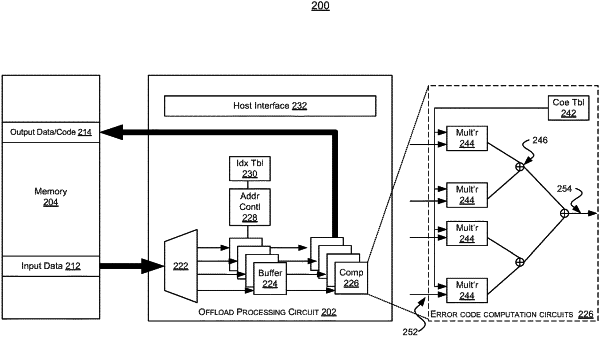
a host interface circuit configured to receive an offloading instruction from a host processing device configured to manage a storage system, wherein the offloading instruction instructs the apparatus to compute an error correction code associated with data elements stored by the storage system;
a memory interface circuit configured to receive the data elements from the storage system; and
an error code computation circuit configured to compute at least a portion of the error correction code, wherein the error code computation circuit is configurable based upon a number of data nodes associated with the data elements.
|