| CPC G06F 11/1004 (2013.01) [G06F 9/30189 (2013.01); G06F 11/0772 (2013.01); G06F 11/108 (2013.01); G06F 11/3037 (2013.01)] | 5 Claims |
|
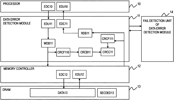
1. A data processing device comprising:
a processor;
a dynamic random access memory (DRAM) whose data is protected by cyclic redundancy check (CRC);
a memory;
an error detection code generation unit (EDC);
an error detection unit (EDU);
first and second CRC function units; and
a flag,
wherein when the flag indicates a first mode:
the processor uses the memory as a cache memory for the DRAM when the processor accesses the DRAM;
data between the processor and the cache memory is protected by both the EDC and the EDU; and
data between the cache memory and the DRAM is protected by the first and second CRC function units,
wherein when the flag indicates a second mode:
the memory operates as a scratchpad memory and not as a cache memory, and the processor accesses the scratchpad memory without accessing the DRAM; and
data between the processor and the scratchpad memory is protected by both the EDC and the EDU,
wherein the memory stores a program for the processor, and
wherein the processor executes the program stored on the memory when the flag indicates the second mode.
|