| CPC G06F 3/0673 (2013.01) [G11C 7/222 (2013.01); H01L 25/0652 (2013.01); H01L 2225/06513 (2013.01); H01L 2225/06541 (2013.01)] | 20 Claims |
|
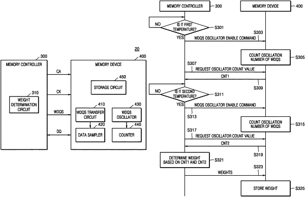
1. A memory system comprising:
a memory device configured to monitor a first oscillator count value for a write data strobe signal for sampling a data signal at a first temperature, and a second oscillator count value for the write data strobe signal for sampling the data signal at a second temperature; and
a memory controller configured to determine a weight based on the first oscillator count value and the second oscillator count value in an initialization process of the memory device or in a test process for the memory device,
wherein the memory device includes a temperature sensor configured to sense a range of temperatures, including the first temperature and the second temperature, of the memory device, and
wherein the memory device is configured to sample the data signal by adjusting a delay on a transfer path of the write data strobe signal according to a sensed temperature of the memory device and the weight.
|