| CPC G06F 3/0631 (2013.01) [G06F 3/0604 (2013.01); G06F 3/0644 (2013.01); G06F 3/0647 (2013.01); G06F 3/0659 (2013.01); G06F 3/0679 (2013.01)] | 14 Claims |
|
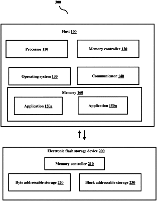
1. A method comprising:
receiving, by a host, a request for memory allocation for a byte addressable storage (ByAS), the receiving being from a first application among a plurality of applications;
detecting applications currently running on a processor of the host from among the plurality of applications;
deallocating, by the host, a least relevant page of a memory space of the ByAs that is allocated to at least one second application among the detected applications while keeping the at least one second application running on the processor, the deallocating based on the request;
moving, by the host, a content to a block addressable storage (BlAS) at a first BlAS location, the content related to the least relevant page, the moving based on the deallocation;
reallocating, by the host, the least relevant page of the memory space to the first application; and
updating, by the host, a cache metadata and a page lookup table of the first application and the at least one second application based on the deallocation and allocation.
|