| CPC G06F 3/0443 (2019.05) [G06F 3/0412 (2013.01); G06V 40/1318 (2022.01); G09G 3/3233 (2013.01); H10K 59/122 (2023.02); H10K 59/1213 (2023.02); H10K 59/131 (2023.02); H10K 59/40 (2023.02); H10K 59/65 (2023.02); G06F 3/0446 (2019.05); G09G 2300/0452 (2013.01); G09G 2300/0819 (2013.01); G09G 2300/0842 (2013.01); G09G 2300/0861 (2013.01); G09G 2354/00 (2013.01); H01L 27/1225 (2013.01); H01L 29/7869 (2013.01); H01L 29/78675 (2013.01)] | 17 Claims |
|
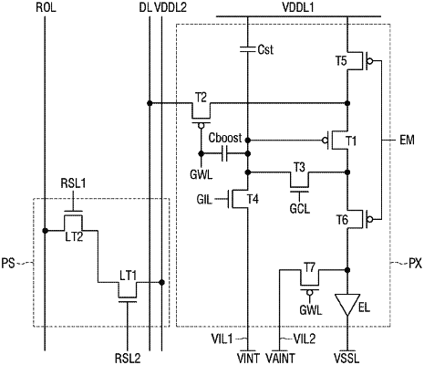
1. A display device comprising:
a substrate;
a plurality of pixels disposed on the substrate and including a first emission area and a second emission area configured to emit light, wherein at least one pixel of the plurality of pixels comprises:
a light emitting element;
a first transistor providing a driving current to the light emitting element and including a first channel, a first electrode, and a second electrode; and
a second transistor electrically connected to the first electrode or the second electrode and including a second channel,
wherein the first channel and the second channel include different materials from each other;
a plurality of optical sensors disposed on the substrate and comprising a light-sensing transistor including a first sensing channel configured to sense light;
a bank disposed on the plurality of pixels and the plurality of optical sensors; and
a touch conductive layer disposed on the bank and including touch electrodes,
wherein the touch conductive layer comprises a light-transmission opening disposed between the first emission area, the second emission area, and the touch electrodes,
wherein the first channel includes polysilicon, and each of the second channel and the first sensing channel include an oxide semiconductor, and
wherein the light-transmission opening overlaps the bank and the light-sensing transistor in a thickness direction of the substrate.
|