| CPC G06F 3/044 (2013.01) [G06F 3/0414 (2013.01); H10N 30/10516 (2023.02); H10N 30/302 (2023.02); H10N 30/852 (2023.02); H10N 30/853 (2023.02); G06F 2203/04105 (2013.01)] | 16 Claims |
|
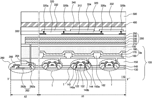
1. A display device, comprising:
a thin film transistor over a substrate;
an overcoat layer on the thin film transistor;
a first electrode on the overcoat layer;
a light-emitting layer on the first electrode;
a second electrode on the light-emitting layer;
an encapsulation layer on the second electrode;
a piezoelectric element over the encapsulation layer;
a touch panel over the piezoelectric element; and
a polarizing plate over the encapsulation layer,
wherein the piezoelectric element includes an upper electrode, a lower electrode, and a piezoelectric layer,
wherein a display area displaying an image and a non-display area surrounding the display area are defined on the substrate, and
wherein each of the lower electrode and the upper electrode has a larger area than a total area of electrodes of the touch panel formed in the display area.
|