| CPC G06F 3/0421 (2013.01) [G06F 3/042 (2013.01); G06F 3/0412 (2013.01); G09G 3/3225 (2013.01); H01L 33/007 (2013.01); H01L 33/20 (2013.01); H01L 33/32 (2013.01); H01L 33/38 (2013.01); G09G 2380/02 (2013.01)] | 15 Claims |
|
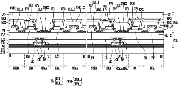
1. A display device comprising:
a substrate; and
a plurality of pixels disposed in the substrate, each of the pixels comprising first and second sub-pixels, each of the first and second sub-pixels having a light emitting region for emitting light,
wherein the first sub-pixel comprises:
a first contact electrode, a second contact electrode, and a third contact electrode disposed on the substrate and spaced apart from each other;
a first light emitting element disposed between the first contact electrode and the second contact electrode and electrically connected to the first contact electrode and the second contact electrode;
a second light emitting element disposed between the second contact electrode and the third contact electrode and electrically connected to the second contact electrode and the third contact electrode;
a first electrode overlapping the first contact electrode on the substrate and adjacent to a first end of the first light emitting element;
a second electrode overlapping the second contact electrode on the substrate and adjacent to a second end of the first light emitting element and a first end of the second light emitting element; and
a third electrode overlapping the third contact electrode on the substrate and adjacent to a second end of the second light emitting element,
wherein the second end of the first light emitting element and the first end of the second light emitting element are electrically connected to the second contact electrode.
|