|
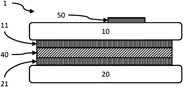
1. Laminated glass pane having a first glass layer and a second glass layer, wherein at least one first electrically conducting structure and a second electrically conducting structure are arranged between the first glass layer and the second glass layer, wherein the first electrically conducting structure and the second electrically conducting structure are arranged spaced apart from one another along a direction perpendicular to a main surface of the first glass layer, with the first electrically conducting structure being arranged in a first plane and the second electrically conducting structure being arranged in a second plane different from the first plane, wherein the first electrically conducting structure at least partially overlaps the second electrically conducting structure in a perpendicular orientation relative to the first glass layer, wherein the first electrically conducting structure constitutes a first electrical element and the second electrically conducting structure constitutes a second electrical element, wherein the first electrical element and the second electrical element are each a capacitive sensor, wherein one of the first electrically conducting structure and the second electrically conducting structure provides a ground potential and the other one of the first electrically conducting structure and the second electrically conducting structure provides a different potential to be measured, and wherein the first electrically conducting structure and the second electrically conducting structure are arranged on at least one inlet, with the first electrically conducting structure being arranged on one side of the inlet and the second electrically conducting structure being arranged on an opposite side of the inlet.
|