| CPC G06F 1/3275 (2013.01) [G05F 3/24 (2013.01); G06F 1/3287 (2013.01); G06F 15/7821 (2013.01); G11C 11/413 (2013.01)] | 19 Claims |
|
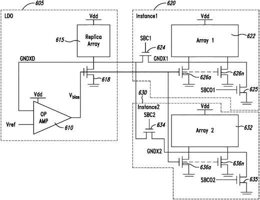
1. A system on chip (SoC) device, comprising:
one or more processors;
a memory coupled to the one or more processors and having a plurality of memory circuits including a first set of memory circuits, wherein each respective memory circuit of the first set of memory circuits is coupled to a respective ballast driver and a respective active memory signal switch for the respective memory circuit; and
a common voltage regulator coupled to a respective gate node of each respective ballast driver for each memory circuit of the plurality of memory circuits, and to a bias node of at least one of the respective memory circuits, wherein the plurality of memory circuits includes an additional memory circuit, a bias node of the additional memory circuit is coupled to a common bias node of the common voltage regulator, and the additional memory circuit, in operation, is maintained in a retention state.
|