| CPC G05F 1/56 (2013.01) [H02M 1/088 (2013.01)] | 19 Claims |
|
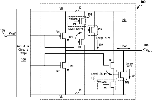
1. Regulator circuitry, comprising:
a first output transistor of a first channel conductivity type, the first output transistor having a drain coupled to an output node on which an output voltage is generated and a source coupled to a first power supply line;
a second output transistor of the first channel conductivity type, the second output transistor having a drain coupled to the output node and a source coupled to the first power supply line, wherein a gate width of the second output transistor is larger than a gate width of the first output transistor;
a third output transistor of a second channel conductivity type opposite to the first channel conductivity type, the third output transistor having a drain coupled to the output node and a source coupled to a second power supply line;
a first control transistor of the first channel conductivity type, the first control transistor having a gate coupled to a gate of the first output transistor and a source coupled to a gate of the second output transistor; and
a circuit stage configured to drive the gates of the first output transistor, the third output transistor, and the first control transistor based on a specified level of the output voltage.
|