US 11,726,406 B2
Method of coating a photoresist and apparatus for performing the same
Sunghwan Kim, Hanam-si (KR); Ho-Young Kim, Seoul (KR); Seok Heo, Hwaseong-si (KR); Dongwook Kim, Seoul (KR); Sungjin Kim, Suwon-si (KR); Chaehung Lim, Hwaseong-si (KR); Jaekyung Park, Seoul (KR); Jae Hong Lee, Seongnam-si (KR); and Junyoung Lee, Yongin-si (KR)
Assigned to Samsung Electronics Co., Ltd., Gyeonggi-do (KR); and Seoul National University R&DB Foundation, Seoul (KR)
Filed by Sunghwan Kim, Hanam-si (KR); Ho-Young Kim, Seoul (KR); Seok Heo, Hwaseong-si (KR); Dongwook Kim, Seoul (KR); Sungjin Kim, Suwon-si (KR); Chaehung Lim, Hwaseong-si (KR); Jaekyung Park, Seoul (KR); Jae Hong Lee, Seongnam-si (KR); and Junyoung Lee, Yongin-si (KR)
Filed on Apr. 12, 2022, as Appl. No. 17/718,648.
Claims priority of application No. 10-2021-0136230 (KR), filed on Oct. 14, 2021.
Prior Publication US 2023/0119739 A1, Apr. 20, 2023
Int. Cl. G03F 7/16 (2006.01); G03F 7/20 (2006.01)
CPC G03F 7/162 (2013.01) [G03F 7/168 (2013.01); G03F 7/2028 (2013.01)] 14 Claims
OG exemplary drawing
 
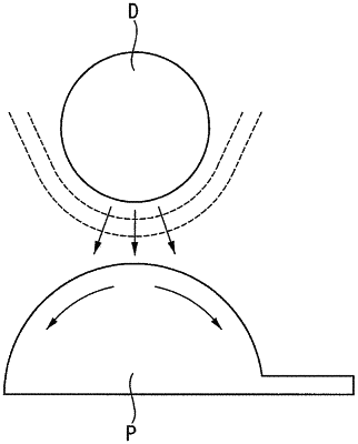
1. A method of coating a photoresist, the method comprising:
providing the photoresist on an upper surface of a wafer, the wafer being rotated; and
injecting a hovering solution toward an edge portion of the photoresist under a hovering condition such that the hovering solution hovers with respect to the edge portion of the photoresist on an edge portion of the upper surface of the wafer with an air layer between the hovering solution and the photoresist to prevent a bead of the photoresist from forming on the edge portion of the upper surface of the wafer.