| CPC G03F 1/38 (2013.01) [G03F 7/091 (2013.01); G03F 7/162 (2013.01); G03F 7/20 (2013.01); G03F 7/26 (2013.01); G03F 7/40 (2013.01); G03F 7/70425 (2013.01); H01L 21/0274 (2013.01)] | 15 Claims |
|
1. A lithography process method for defining sidewall morphology of a lithography pattern, comprising the following steps:
Step 1: designing a mask and forming a tangible mask according to a design, wherein a mask pattern is formed on the tangible mask, the mask pattern being used to define a lithography pattern;
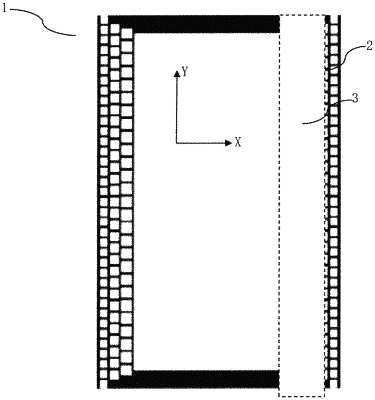
the lithography pattern has a sidewall, and a mask side face pattern structure that defines sidewall morphology of the lithography pattern is provided on the mask pattern, the mask side face pattern structure having a structure that enables an exposure light intensity to gradually change, wherein in an area of a larger exposure light intensity, the height of the sidewall of the lithography pattern is smaller, and in an area of a smaller exposure light intensity, the height of the sidewall of the lithography pattern is larger;
the mask side face pattern structure has a plurality of first hollow structures in the shape of holes or slits in a top view, there is a first solid structure between the first hollow structures; or,
the mask side face pattern structure has a plurality of second solid structures in the shape of holes or slits in a top view, there is a second hollow structure between the second solid structures;
Step 2: coating a to-be-exposed substrate with a photoresist;
Step 3: exposing the photoresist by using the mask, and then developing the photoresist to form the lithography pattern, wherein during an exposure process, the mask side face pattern structure defines the sidewall morphology of the lithography pattern by enabling the exposure light intensity to gradually change; and
Step 4: post-exposure-baking the photoresist.
|