US 11,726,398 B2
Method for inspecting a reticle, a method for manufacturing a reticle, and a method for manufacturing a semiconductor device using the same
Seulgi Kim, Hwaseong-si (KR); Hyonseok Song, Suwon-si (KR); Inyong Kang, Seoul (KR); Kangwon Lee, Hwaseong-si (KR); JuHyoung Lee, Hwaseong-si (KR); and Eunsik Jang, Seoul (KR)
Assigned to Samsung Electronics Co., Ltd., Gyeonggi-do (KR)
Filed by Samsung Electronics Co., Ltd., Suwon-si (KR)
Filed on Jul. 27, 2022, as Appl. No. 17/874,783.
Application 17/874,783 is a division of application No. 16/800,316, filed on Feb. 25, 2020, granted, now 11,467,484.
Claims priority of application No. 10-2019-0093406 (KR), filed on Jul. 31, 2019.
Prior Publication US 2022/0365415 A1, Nov. 17, 2022
Int. Cl. G03F 1/22 (2012.01); G03F 7/20 (2006.01); H01L 21/66 (2006.01); H01L 21/027 (2006.01); G01N 21/956 (2006.01)
CPC G03F 1/22 (2013.01) [G03F 7/2004 (2013.01); H01L 21/0274 (2013.01); H01L 22/12 (2013.01); G01N 2021/95676 (2013.01)] 10 Claims
OG exemplary drawing
 
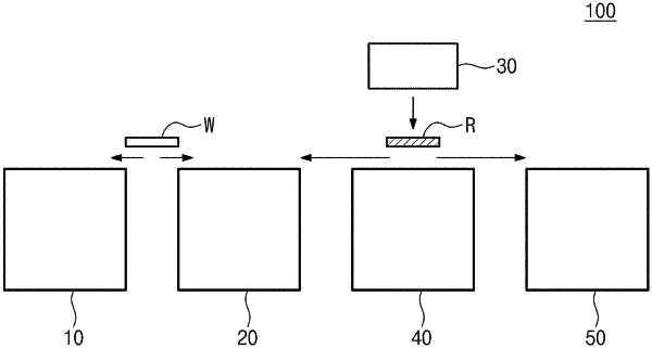
1. A method for manufacturing a reticle, the method comprising:
forming a reflective layer on a reticle substrate; and
inspecting the reflective layer,
the inspecting of the reflective layer including,
cooling the reticle substrate,
irradiating a laser beam to the reflective layer, and
receiving the laser beam using a photodetector to obtain an image of the reflective layer; and
detecting whether a defect in the reflective layer exists based on the image of the reflective layer;
wherein the reticle substrate is cooled to below 145 kelvins (K) to decrease a specific heat capacity of the reflective layer and to increase a power of the laser beam.