| CPC G02F 1/1368 (2013.01) [G02F 1/1339 (2013.01); G02F 1/133345 (2013.01); G02F 1/134309 (2013.01); G02F 1/136286 (2013.01); H01L 27/1214 (2013.01); H01L 27/1222 (2013.01); H01L 27/1288 (2013.01); H01L 29/04 (2013.01); H01L 29/66765 (2013.01); H01L 29/78678 (2013.01); H01L 29/78696 (2013.01); H01L 29/458 (2013.01); H01L 29/4908 (2013.01)] | 10 Claims |
|
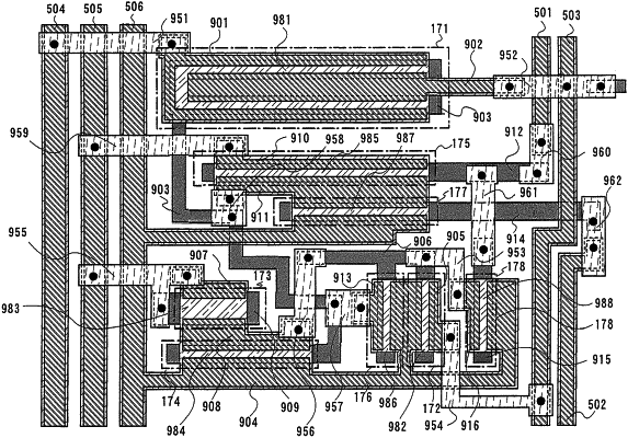
1. A liquid crystal display device comprising:
a pixel comprising a first pixel electrode of a first liquid crystal element and a second pixel electrode of a second liquid crystal element; and
a shift register electrically connected to the pixel, the shift register comprising a first transistor, a second transistor, a third transistor, and a fourth transistor,
wherein each of the first pixel electrode and the second pixel electrode is a sub-pixel,
wherein one of a source electrode and a drain electrode of the first transistor is electrically connected to one of a source electrode and a drain electrode of the second transistor,
wherein one of a source electrode and a drain electrode of the third transistor is electrically connected to one of a source electrode and a drain electrode of the fourth transistor,
wherein the other of the source electrode and the drain electrode of the first transistor is electrically connected to a first wiring,
wherein the other of the source electrode and the drain electrode of the second transistor is electrically connected to a second wiring,
wherein a gate electrode of the first transistor is electrically connected to a gate electrode of the fourth transistor,
wherein a gate electrode of the second transistor is electrically connected to the one of the source electrode and the drain electrode of the third transistor and the one of the source electrode and the drain electrode of the fourth transistor,
wherein a gate electrode of the third transistor is electrically connected to the other of the source electrode and the drain electrode of the third transistor,
wherein each of the first transistor, the second transistor, the third transistor, and the fourth transistor includes:
a gate insulating film over the gate electrode;
a first semiconductor film over the gate insulating film;
a second semiconductor film over the first semiconductor film;
a third semiconductor film over the second semiconductor film; and
the source electrode and the drain electrode over the third semiconductor film, and
wherein an end portion of one of the source electrode and the drain electrode included in one of the first transistor, the second transistor, the third transistor, and the fourth transistor has a region positioned inside an end portion of the third semiconductor film included in the one of the first transistor, the second transistor, the third transistor, and the fourth transistor.
|