| CPC G02F 1/1368 (2013.01) [G02F 1/13439 (2013.01); G02F 1/136277 (2013.01); G02F 1/136286 (2013.01); H01L 27/1225 (2013.01); H01L 27/1251 (2013.01); H01L 29/78648 (2013.01); G02F 1/13338 (2013.01); G02F 1/13454 (2013.01); G02F 1/13685 (2021.01); G02F 1/133388 (2021.01); G02F 1/136295 (2021.01); G02F 2202/103 (2013.01); G02F 2202/104 (2013.01)] | 18 Claims |
|
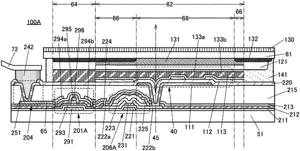
1. A display device comprising:
a display portion; and
a driver circuit portion,
wherein the display portion comprises a liquid crystal element, a first transistor, a scan line, and a signal line,
wherein the driver circuit portion comprises a second transistor,
wherein the liquid crystal element comprises a pixel electrode, a liquid crystal layer, and a common electrode,
wherein each of the scan line and the signal line is electrically connected to the first transistor,
wherein the scan line and the signal line each comprise a metal layer,
wherein a structure of the first transistor is different from a structure of the second transistor,
wherein each of a first semiconductor layer of the first transistor and a second semiconductor layer of the second transistor is provided over and in direct contact with a first insulating layer,
wherein the first semiconductor layer comprises a first metal oxide,
wherein the second semiconductor layer comprises a second metal oxide,
wherein the first transistor comprises a first region directly connected to the pixel electrode,
wherein the second transistor comprises a second insulating layer over the second semiconductor layer and a first upper gate electrode over the second insulating layer,
wherein the first upper gate electrode comprises an oxide conductor comprising an impurity element,
wherein an upper end of a side surface of the second insulating layer and a lower end of a side surface of the first upper gate electrode coincide with each other,
wherein each of the pixel electrode, the common electrode, and the first region comprises a conductive material transmitting visible light, and
wherein visible light passes through the first region and the liquid crystal element and is emitted to an outside of the display device.
|