| CPC G02F 1/13452 (2013.01) [G02F 1/1339 (2013.01); G02F 1/1341 (2013.01); G02F 1/1368 (2013.01); G02F 1/13306 (2013.01); G02F 1/13394 (2013.01); G02F 1/133345 (2013.01); G02F 1/133512 (2013.01); G02F 1/133514 (2013.01); G09G 3/20 (2013.01); G09G 3/2092 (2013.01); H01L 27/1222 (2013.01); H05K 1/117 (2013.01); H05K 1/148 (2013.01); H05K 3/361 (2013.01); G09G 3/3614 (2013.01); G09G 2300/0408 (2013.01); G09G 2300/0426 (2013.01); G09G 2300/0439 (2013.01); G09G 2300/08 (2013.01); G09G 2310/0264 (2013.01); G09G 2320/043 (2013.01); G09G 2330/021 (2013.01); G09G 2330/08 (2013.01); H01L 2924/0002 (2013.01); H05K 1/0263 (2013.01); H05K 1/0265 (2013.01); H05K 2201/094 (2013.01); H05K 2201/09727 (2013.01); H05K 2201/10136 (2013.01); H05K 2201/10166 (2013.01)] | 3 Claims |
|
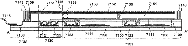
1. A semiconductor device comprising:
a sealing material;
a plurality of scan line driver circuits;
a connection terminal portion, comprising a plurality of connection pads, over a first substrate;
a plurality of wirings electrically connected to each of the plurality of connection pads; and
a pixel portion including a transistor and a display element, the transistor comprising:
a gate electrode over the first substrate;
a semiconductor layer over and overlapping with the gate electrode; and
a first conductive layer and a second conductive layer electrically connected to the semiconductor layer,
wherein the second conductive layer is electrically connected to a first pixel electrode of the display element,
wherein a color filter overlapping with the display element is provided on the first substrate side,
wherein a spacer is provided over the color filter and the first pixel electrode,
wherein the plurality of connection pads have a similar width,
wherein the plurality of wirings are arranged at substantially regular intervals,
wherein the plurality of scan line driver circuits is provided over the first substrate,
wherein the sealing material surrounds the pixel portion and the plurality of scan line driver circuits,
wherein the sealing material does not surround the plurality of connection pads,
wherein the plurality of wirings comprises a first region not overlapping the sealing material,
wherein the plurality of wirings comprises a second region overlapping the sealing material,
wherein the first conductive layer and the second conductive layer comprise copper,
wherein the first substrate comprises glass,
wherein the gate electrode comprises copper,
wherein the first pixel electrode comprises indium, tin, and oxygen, and
wherein the semiconductor layer comprises amorphous silicon.
|