US 11,726,371 B2
FFS-mode liquid crystal display device comprising a top-gate transistor and an auxiliary wiring connected to a common electrode in a pixel portion
Hajime Kimura, Kanagawa (JP)
Assigned to Semiconductor Energy Laboratory Co., Ltd., Atsugi (JP)
Filed by Semiconductor Energy Laboratory Co., Ltd., Atsugi (JP)
Filed on Jul. 9, 2021, as Appl. No. 17/371,944.
Application 17/371,944 is a continuation of application No. 16/714,866, filed on Dec. 16, 2019, granted, now 11,061,285.
Application 16/714,866 is a continuation of application No. 16/520,560, filed on Jul. 24, 2019, granted, now 10,509,271, issued on Dec. 17, 2019.
Application 16/520,560 is a continuation of application No. 16/378,632, filed on Apr. 9, 2019, granted, now 11,435,626.
Application 16/378,632 is a continuation of application No. 16/009,973, filed on Jun. 15, 2018, granted, now 11,106,096.
Application 16/009,973 is a continuation of application No. 15/649,756, filed on Jul. 14, 2017, granted, now 10,001,678, issued on Jun. 19, 2018.
Application 15/649,756 is a continuation of application No. 15/047,844, filed on Feb. 19, 2016, granted, now 9,709,861, issued on Jul. 18, 2017.
Application 15/047,844 is a continuation of application No. 14/492,136, filed on Sep. 22, 2014, granted, now 9,268,188, issued on Feb. 23, 2016.
Application 14/492,136 is a continuation of application No. 14/013,292, filed on Aug. 29, 2013, granted, now 8,841,671, issued on Sep. 23, 2014.
Application 14/013,292 is a continuation of application No. 13/723,332, filed on Dec. 21, 2012, granted, now 8,872,182, issued on Oct. 28, 2014.
Application 13/723,332 is a continuation of application No. 12/900,612, filed on Oct. 8, 2010, granted, now 8,338,865, issued on Dec. 25, 2012.
Application 12/900,612 is a continuation of application No. 11/746,377, filed on May 9, 2007, granted, now 7,816,682, issued on Oct. 19, 2010.
Claims priority of application No. 2006-135954 (JP), filed on May 16, 2006.
Prior Publication US 2021/0333653 A1, Oct. 28, 2021
Int. Cl. G02F 1/1343 (2006.01); G02F 1/1362 (2006.01); G02F 1/1337 (2006.01); G02F 1/136 (2006.01); G02F 1/1333 (2006.01); G02F 1/1368 (2006.01)
CPC G02F 1/134372 (2021.01) [G02F 1/136 (2013.01); G02F 1/1337 (2013.01); G02F 1/1368 (2013.01); G02F 1/13439 (2013.01); G02F 1/133345 (2013.01); G02F 1/133707 (2013.01); G02F 1/134309 (2013.01); G02F 1/134363 (2013.01); G02F 1/136227 (2013.01); G02F 1/136277 (2013.01); G02F 1/136286 (2013.01); G02F 1/13685 (2021.01); G02F 1/134318 (2021.01); G02F 2201/121 (2013.01)] 10 Claims
OG exemplary drawing
 
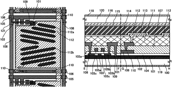
1. An FFS-mode liquid crystal display device comprising:
an auxiliary wiring electrically connected to a common electrode in a pixel portion and comprising a region arranged parallel or substantially parallel to a source wiring in a plan view of the pixel portion;
a top-gate transistor electrically connected to the source wiring;
a pixel electrode electrically connected to the top-gate transistor and comprising a plurality of openings;
a first organic insulating film below the source wiring; and
a second organic insulating film over the source wiring,
wherein each of the common electrode and the pixel electrode comprises indium tin oxide or indium zinc oxide, and
wherein the auxiliary wiring comprises one or more element selected from aluminum, tantalum, titanium, molybdenum, tungsten, neodymium, chromium, nickel, platinum, gold, silver, copper, magnesium, scandium, and cobalt.