| CPC G02F 1/0063 (2013.01) [G02F 1/133502 (2013.01); G02F 1/133514 (2013.01); G02F 1/133516 (2013.01); G02F 1/133617 (2013.01); G02F 1/133707 (2013.01); G02F 1/133357 (2021.01); G02F 1/133548 (2021.01); G02F 1/133565 (2021.01); G02F 1/136281 (2021.01); G02F 2001/1635 (2013.01); G02F 2201/48 (2013.01); G02F 2203/055 (2013.01)] | 9 Claims |
|
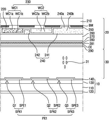
1. A display device comprising:
a substrate;
a color conversion layer disposed on the substrate and comprising a first wavelength conversion layer configured to receive a light of a first wavelength range and to convert the light of the first wavelength range into a light of a second wavelength range, and a second wavelength conversion layer configured to receive the light of the first wavelength range and to convert the light of the first wavelength range into a light of a third wavelength range;
a filter disposed on the color conversion layer and configured to transmit the light of the first wavelength range and to reflect the light of the second wavelength range and the light of the third wavelength range;
a transmissive layer disposed on the filter and configured to transmit the light of the first wavelength range; and
a planarization layer disposed on the transmissive layer,
wherein:
the transmissive layer is disposed between the filter and the planarization layer;
a portion of the filter is disposed between the transmissive layer and the substrate; and
the first wavelength conversion layer and the second wavelength conversion layer are disposed between the filter and the substrate.
|