US 11,726,342 B2
Multifunctional collimator for contact image sensors
Hsin-Yu Chen, Hsinchu (TW); Chun-Peng Li, Hsinchu (TW); Chia-Chun Hung, Hsinchu (TW); Ching-Hsiang Hu, Taipei (TW); Wei-Ding Wu, Zhubei (TW); Jui-Chun Weng, Taipei (TW); Ji-Hong Chiang, Changhua (TW); Yen Chiang Liu, Hsinchu (TW); Jiun-Jie Chiou, Hsinchu (TW); Li-Yang Tu, Hsinchu (TW); Jia-Syuan Li, Hsinchu (TW); You-Cheng Jhang, Hsinchu (TW); Shin-Hua Chen, Hsinchu (TW); Lavanya Sanagavarapu, Hsinchu (TW); Han-Zong Pan, Hsinchu (TW); and Hsi-Cheng Hsu, Taichung (TW)
Assigned to Taiwan Semiconductor Manufacturing Co., Ltd., Hsin-Chu (TW)
Filed by Taiwan Semiconductor Manufacturing Co., Ltd., Hsin-Chu (TW)
Filed on Aug. 4, 2022, as Appl. No. 17/881,439.
Application 17/881,439 is a continuation of application No. 16/655,763, filed on Oct. 17, 2019, granted, now 11,448,891.
Prior Publication US 2022/0373815 A1, Nov. 24, 2022
This patent is subject to a terminal disclaimer.
Int. Cl. G02B 27/30 (2006.01); H01L 31/0232 (2014.01); H01L 27/146 (2006.01)
CPC G02B 27/30 (2013.01) [H01L 27/14625 (2013.01); H01L 31/02325 (2013.01)] 20 Claims
OG exemplary drawing
 
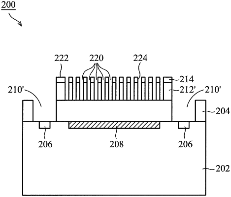
1. An optical collimator, comprising:
a dielectric layer;
a substrate; and
a plurality of via holes,
wherein the dielectric layer is formed over the substrate, wherein the plurality of via holes are configured as an array along a lateral direction of a first surface of the dielectric layer, wherein each of the plurality of via holes extends through the dielectric layer and the substrate from the first surface of the dielectric layer to a second surface of the substrate in a vertical direction, wherein a bulk impurity doping concentration and a first thickness of the substrate are configured so as to allow the optical collimator to filter light in a range of wavelengths between 780 and 1100 nanometers.