| CPC G02B 15/00 (2013.01) [G02B 3/14 (2013.01); G02B 26/005 (2013.01); H04N 23/69 (2023.01); H04N 23/951 (2023.01); H04N 23/51 (2023.01)] | 24 Claims |
|
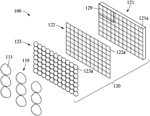
1. An imaging device comprising:
a plurality of imaging lens arrays comprising a plurality of imaging optical lenses; and
a sensing array comprising a plurality of sensing elements configured to sense light passing through the plurality of imaging lens arrays,
wherein the plurality of imaging lens arrays comprises a first imaging lens array and a second imaging lens array arranged in different planes in an optical axis, and
wherein the first imaging lens array comprises an active imaging lens with a variable focal length.
|