US 11,726,207 B2
Imaging device and method
Alper Ercan, Stuttgart (DE); Michiel Timmermans, Stuttgart (DE); and Ward Van Der Tempel, Stuttgart (DE)
Assigned to Sony Semiconductor Solutions Corporation, Kanagawa (JP)
Appl. No. 16/954,180
Filed by Sony Semiconductor Solutions Corporation, Kanagawa (JP)
PCT Filed Dec. 21, 2018, PCT No. PCT/EP2018/086736
§ 371(c)(1), (2) Date Jun. 15, 2020,
PCT Pub. No. WO2019/129740, PCT Pub. Date Jul. 4, 2019.
Claims priority of application No. 17211206 (EP), filed on Dec. 29, 2017.
Prior Publication US 2021/0157005 A1, May 27, 2021
Int. Cl. G01S 17/36 (2006.01); G01S 17/894 (2020.01); G01S 7/4915 (2020.01)
CPC G01S 17/36 (2013.01) [G01S 7/4915 (2013.01); G01S 17/894 (2020.01)] 18 Claims
OG exemplary drawing
 
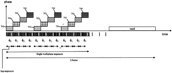
1. An electronic device comprising circuitry configured to accumulate, in a multiphase exposure, first phase data from a first sub-exposure with second phase data which is based on a same correlation phase and is from a second sub-exposure, in an associated phase memory.