| CPC G01R 31/318541 (2013.01) [G11C 7/106 (2013.01); G11C 7/1087 (2013.01); G11C 7/222 (2013.01); H03K 3/0372 (2013.01); H03K 19/20 (2013.01)] | 20 Claims |
|
1. A flip-flop circuit, comprising:
a clock generator configured to generate a plurality of clock signals; and
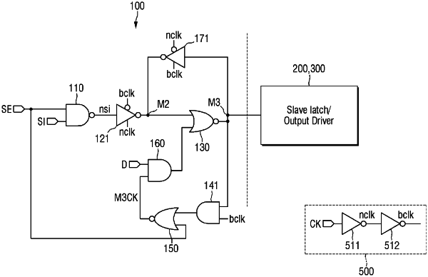
a master-slave latch circuit including a master latch and a slave latch, said master latch comprising:
a scan path configured to output a scan path signal in response to a scan enable signal and a scan input signal;
a data path configured to output a first latch signal in response to performing an operation on a data signal and the scan path signal, which is a function of the plurality of clock signals; and
a feedback path comprising a first tri-state inverter, which is connected between an output terminal of the data path and an output terminal of the scan path, said feedback path configured to feed back the first latch signal of a previous state according to the plurality of clock signals;
wherein the data signal is input to the data path independently of the scan path.
|