| CPC G01R 31/3177 (2013.01) [G01R 31/31724 (2013.01); G01R 31/31727 (2013.01); G06F 1/04 (2013.01)] | 21 Claims |
|
1. A method for detecting faults in an integrated circuit (IC), the method comprising:
entering scan mode of the IC;
receiving, at the IC, a test pattern;
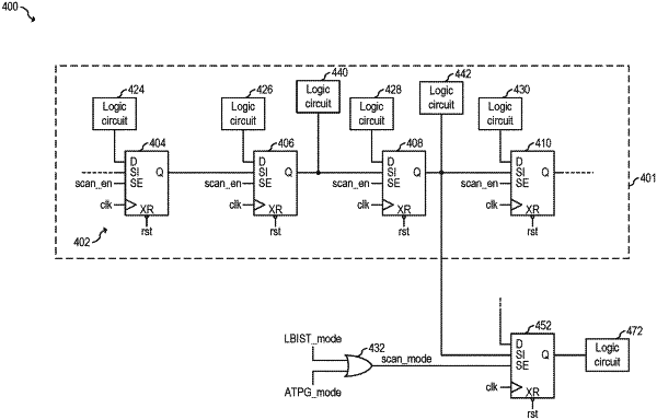
applying, at the IC, the test pattern through a first scan chain by asserting and deasserting a scan enable signal to respectively perform shift and capture operations to the first scan chain;
while applying the test pattern through the first scan chain, controlling, at the IC, a further scan flip-flop with the first scan chain without transitioning a further scan enable input of the further scan flip-flop; and
evaluating an output of the first scan chain to detect faults in the IC.
|