| CPC G01P 21/00 (2013.01) | 8 Claims |
|
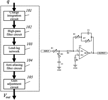
1. A signal conditioning system for low-frequency measurement of an acceleration sensor, comprising: a charge integration circuit, a high-pass filter circuit, a lead-lag network, an anti-aliasing filter circuit, and a gain adjustment circuit;
an input terminal of the charge integration circuit is connected to the acceleration sensor, an output terminal of the charge integration circuit is connected to an input terminal of the high-pass filter circuit, an output terminal of the high-pass filter circuit is connected to an input terminal of the lead-lag network, an output terminal of the lead-lag network is connected to an input terminal of the anti-aliasing filter circuit, and an output terminal of the anti-aliasing filter circuit is connected to an input terminal of the gain adjustment circuit;
the charge integration circuit is used to convert a charge signal generated by measurement of the acceleration sensor into a voltage signal for operational amplification; the high-pass filter circuit is used to filter a direct current (DC) component in the voltage signal for the operational amplification; the lead-lag network is used to expand a measurement bandwidth of the acceleration sensor to a low-frequency band; the anti-aliasing filter circuit is used to adjust a constraint bandwidth of an output signal; and the gain adjustment circuit is used to adjust an output gain of the output signal;
the lead-lag network comprises: a second resistor, a third resistor, a third capacitor, a fourth resistor, a fifth resistor, a sixth resistor, a seventh resistor, a fourth capacitor, and a third operational amplifier; and the second resistor, the third resistor, the fifth resistor, and the seventh resistor are all adjustable resistors; and
an input terminal of the second resistor is connected to the output terminal of the high-pass filter circuit, an output terminal of the second resistor is connected to an input terminal of the third resistor and an input terminal of the fourth resistor respectively, an output terminal of the third resistor is connected to an input terminal of the third capacitor, an output terminal of the third capacitor is grounded, an output terminal of the fourth resistor is connected to an input terminal of the fifth resistor and a second input terminal of the third operational amplifier respectively, an output terminal of the fifth resistor is connected to an input terminal of the seventh resistor and an input terminal of the fourth capacitor respectively, an output terminal of the seventh resistor and an output terminal of the fourth capacitor are both connected to an output terminal of the third operational amplifier, the output terminal of the third operational amplifier is further connected to the anti-aliasing filter circuit, one terminal of the sixth resistor is connected to a first input terminal of the third operational amplifier, and the other terminal of the sixth resistor is grounded.
|