| CPC G01N 27/4145 (2013.01) | 11 Claims |
|
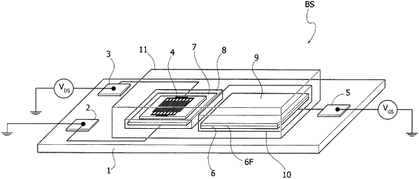
1. A field effect transistor sensor including:
a substrate;
a source electrode;
a drain electrode;
a gate electrode functionalized with a layer of biological recognition elements;
a source-drain channel;
a semiconductor layer; and
the layer of biological recognition elements patterned into a plurality of uncoupled domains, such that a surface of the gate electrode is divided into areas of said biological recognition elements;
wherein each domain of said plurality of domains are chemically decoupled from each other domain of said plurality of domains, whereby a chemical change in a first domain of said plurality of domains due to a ligand recognition event is confined within said first domain;
wherein the plurality of domains are arranged according to a matrix; and
wherein each domain of said plurality of domains has a surface extension ranging from 10−7-10−4 cm2 to 10−5-10−1 cm2.
|