US 11,725,992 B2
Sensor, inputting device, and electronic apparatus
Ken Kobayashi, Kanagawa (JP); Akira Ebisui, Kanagawa (JP); Yoshiaki Sakakura, Kanagawa (JP); Tomoko Katsuhara, Kanagawa (JP); Hayato Hasegawa, Kanagawa (JP); and Manami Miyawaki, Kanagawa (JP)
Assigned to SONY CORPORATION, Tokyo (JP)
Appl. No. 16/958,504
Filed by SONY CORPORATION, Tokyo (JP)
PCT Filed Dec. 28, 2018, PCT No. PCT/JP2018/048434
§ 371(c)(1), (2) Date Jun. 26, 2020,
PCT Pub. No. WO2019/135401, PCT Pub. Date Jul. 11, 2019.
Claims priority of application No. 2018-000815 (JP), filed on Jan. 5, 2018.
Prior Publication US 2020/0348191 A1, Nov. 5, 2020
Int. Cl. G01L 1/14 (2006.01); G06F 3/044 (2006.01)
CPC G01L 1/142 (2013.01) [G06F 3/0445 (2019.05); G06F 2203/04102 (2013.01)] 20 Claims
OG exemplary drawing
 
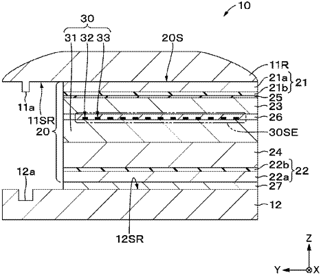
1. A sensor, comprising:
a capacitive sensor electrode layer;
a first reference electrode layer; and
an elastic layer provided between the capacitive sensor electrode layer and the first reference electrode layer, wherein the elastic layer includes a conductive material with a density distribution that decreases from the first reference electrode layer towards the capacitive sensor electrode layer,
a thickness of the elastic layer is 100 μm or less, and
a weight per unit area of the elastic layer is less than 3 mg/cm2.