US 11,725,941 B2
Sensing device
Amir Rahafrooz, Shaker Heights, OH (US); Diego Emilio Serrano, Peachtree City, GA (US); and Ijaz Hussain Jafri, Holliston, MA (US)
Assigned to PANASONIC INTELLECTUAL PROPERTY MANAGEMENT CO., LTD., Osaka (JP)
Appl. No. 17/420,751
Filed by Panasonic Intellectual Property Management Co., Ltd., Osaka (JP)
PCT Filed Dec. 27, 2019, PCT No. PCT/JP2019/051459
§ 371(c)(1), (2) Date Jul. 6, 2021,
PCT Pub. No. WO2020/145203, PCT Pub. Date Jul. 16, 2020.
Claims priority of provisional application 62/789,550, filed on Jan. 8, 2019.
Claims priority of provisional application 62/789,549, filed on Jan. 8, 2019.
Claims priority of provisional application 62/789,548, filed on Jan. 8, 2019.
Prior Publication US 2022/0107181 A1, Apr. 7, 2022
Prior Publication US 2022/0316881 A9, Oct. 6, 2022
Int. Cl. G01C 19/5712 (2012.01); G01P 1/00 (2006.01); G01P 15/125 (2006.01)
CPC G01C 19/5712 (2013.01) [G01P 1/00 (2013.01); G01P 15/125 (2013.01)] 17 Claims
OG exemplary drawing
 
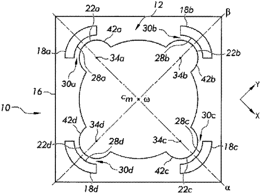
1. A sensing device comprising:
a resonant member that is movable in a first mode and a second mode; and
an electrode,
wherein the resonant member has a capacitive surface portion that faces and is capacitively coupled to a capacitive surface portion of the electrode,
wherein displacement for each point along the capacitive surface portion of the resonant member in the first mode is substantially tangent to the point.