| CPC C23C 14/545 (2013.01) [C23C 14/3492 (2013.01); H01L 27/1244 (2013.01); Y10T 428/12493 (2015.01)] | 7 Claims |
|
1. An electronic device, comprising:
an array substrate, comprising:
a substrate, having a substrate surface;
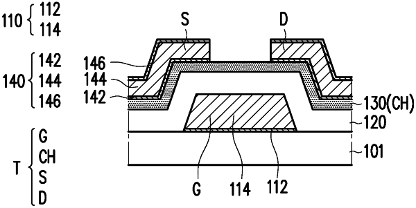
a first conductive layer, located on the substrate surface;
a first insulating layer, located on the first conductive layer;
a second conductive layer, located on the first insulating layer and comprising a first sputtering layer, a second sputtering layer, and a third sputtering layer; and
a second insulating layer, located on the second conductive layer, wherein:
the second sputtering layer is located between the first sputtering layer and the third sputtering layer;
the second sputtering layer comprises a first metal element;
the first sputtering layer comprises the first metal element and a second metal element; and
the third sputtering layer comprises the first metal element and a third metal element,
wherein the array substrate further comprises a semiconductor layer, and the substrate comprises an active area and an inactive area, wherein:
within a range corresponding to the inactive area, at least part of the second conductive layer constitutes a connection pad;
within a range corresponding to the active area, at least part of the first conductive layer, a part of the semiconductor layer, and a part of the second conductive layer constitute an active element; and
within the range corresponding to the inactive area, a part of the second conductive layer is embedded in the first insulating layer to constitute a conducting structure electrically connected to a part of the first conductive layer.
|