| CPC C23C 14/3464 (2013.01) [C23C 14/08 (2013.01); C23C 14/352 (2013.01); H01J 37/32082 (2013.01); H01J 37/32155 (2013.01); H01J 37/32715 (2013.01); H01J 37/3417 (2013.01)] | 10 Claims |
|
1. A method for fabricating a semiconductor device, the method comprising:
forming a first magnetic film on a substrate;
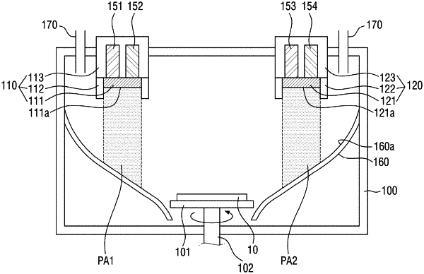
loading the substrate having the first magnetic film on a stage, which is in an inside of a chamber;
providing a first power having a first frequency to a first sputter gun;
providing a first sputtering source generated from the first sputter gun to a projection area on a chamber shield, which is in the inside of the chamber and is included from an upper surface of a side wall of the chamber toward the stage, the projection area being spaced apart from the stage in a horizontal direction and not overlapping the stage in a vertical direction;
depositing an insulation film on the first magnetic film by using the first sputtering source;
unloading the substrate from the chamber;
providing a second power having a second frequency to the first sputter gun, the second frequency being higher than the first frequency; and
cleaning a lower surface of a target exposed at a lower portion of the first sputter gun by using the second power,
wherein at least part of the chamber shield overlaps the stage in the horizontal direction.
|