| CPC H10K 59/131 (2023.02) [H01L 29/78645 (2013.01); H10K 50/822 (2023.02); H10K 50/844 (2023.02); H10K 59/124 (2023.02); H10K 59/1216 (2023.02); H10K 71/00 (2023.02); H10K 71/621 (2023.02); H01L 27/124 (2013.01); H10K 50/813 (2023.02); H10K 59/1201 (2023.02); H10K 59/1213 (2023.02)] | 36 Claims |
|
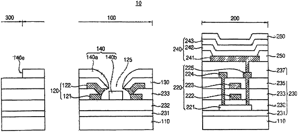
[ 9. An organic light emitting display (OLED) device, comprising a display region, an opening region inside the display region, and a boundary region between the display region and the opening region,
wherein the boundary region comprises:
an insulation layer disposed on a substrate, the insulation layer including a first region and a second region adjacent to the first region;
a conductive layer comprising at least two layers disposed between the insulation layer in the first region and a pixel electrode in the display region and including at least one of titanium (Ti) and aluminum (Al); and
a common layer disposed on the conductive layer that is disposed over the insulation layer in the first region and on the insulation layer in the second region, and
wherein the common layer disposed on the conductive layer that is disposed over the insulation layer in the first region is disconnected from the common layer disposed on the insulation layer in the second region. ]
|