| CPC H10N 70/8833 (2023.02) [H10B 63/80 (2023.02); H10N 70/028 (2023.02); H10N 70/24 (2023.02); H10N 70/826 (2023.02); H10N 70/8265 (2023.02); H10N 70/841 (2023.02)] | 10 Claims |
|
1. A method for fabricating memory device, comprising:
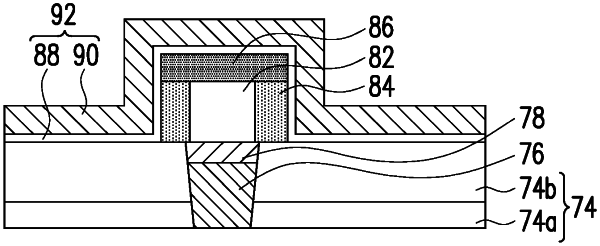
providing a substrate, having a bottom electrode layer therein;
forming a buffer layer and a mask layer on the buffer layer over the substrate, wherein the buffer layer is in contact with the bottom electrode layer, and a top surface of the bottom electrode layer is covered by the buffer layer;
performing an oxidation process on a peripheral portion of the buffer layer to form the peripheral portion of the buffer layer into a resistive layer, wherein the resistive layer laterally surrounds a remaining portion of the buffer layer after the oxidation process and extends upward vertically from the substrate; and
forming, over the substrate, a noble metal layer and a top electrode layer on the noble metal layer, fully covering the resistive layer and the mask layer.
|