| CPC H10N 70/8416 (2023.02) [H10N 70/023 (2023.02); H10B 63/30 (2023.02); H10B 63/80 (2023.02); H10N 70/063 (2023.02); H10N 70/24 (2023.02); H10N 70/826 (2023.02)] | 20 Claims |
|
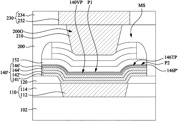
1. A method for fabricating a memory device, comprising:
forming a bottom electrode via in a dielectric layer over a substrate;
depositing a bottom electrode layer over the substrate, wherein the bottom electrode layer comprises a non-noble metal layer and a noble metal layer over the non-noble metal layer, and each of the non-noble metal layer and the noble metal layer comprises a first portion over the bottom electrode via and a second portion over the dielectric layer;
depositing a buffer layer over the first and second portions of the noble metal layer of the bottom electrode layer;
performing a surface treatment to a top surface of the buffer layer;
depositing a resistance switch layer over the top surface of the buffer layer after performing the surface treatment;
forming a top electrode over the resistance switch layer; and
patterning the resistance switch layer into a resistance switch element below the top electrode.
|