| CPC H10N 70/8265 (2023.02) [H10B 63/30 (2023.02); H10N 70/011 (2023.02); H10N 70/063 (2023.02); H10N 70/066 (2023.02); H10N 70/20 (2023.02); H10N 70/24 (2023.02); H10N 70/826 (2023.02); H10N 70/841 (2023.02); H10N 70/8833 (2023.02); H10N 70/021 (2023.02); H10N 70/023 (2023.02); H10N 70/026 (2023.02); H10N 70/028 (2023.02); H10N 70/041 (2023.02); H10N 70/043 (2023.02); H10N 70/046 (2023.02); H10N 70/061 (2023.02); H10N 70/068 (2023.02); H10N 70/231 (2023.02); H10N 70/235 (2023.02); H10N 70/245 (2023.02); H10N 70/25 (2023.02); H10N 70/253 (2023.02); H10N 70/257 (2023.02); H10N 70/801 (2023.02); H10N 70/821 (2023.02); H10N 70/823 (2023.02); H10N 70/828 (2023.02); H10N 70/8413 (2023.02); H10N 70/8416 (2023.02); H10N 70/8418 (2023.02); H10N 70/8613 (2023.02); H10N 70/8616 (2023.02); H10N 70/881 (2023.02); H10N 70/882 (2023.02); H10N 70/883 (2023.02); H10N 70/884 (2023.02); H10N 70/8822 (2023.02); H10N 70/8825 (2023.02); H10N 70/8828 (2023.02); H10N 70/8836 (2023.02); H10N 70/8845 (2023.02)] | 20 Claims |
|
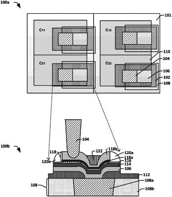
1. A memory device, comprising:
a dielectric protection layer having sidewalls defining an opening over a conductive interconnect within an inter-level dielectric (ILD) layer;
a bottom electrode structure extending from within the opening to directly over a topmost surface of the dielectric protection layer facing away from the ILD layer, wherein the bottom electrode structure has one or more rounded sidewalls that are vertically between a topmost surface of the bottom electrode structure and a recessed upper surface of the bottom electrode structure that faces away from the conductive interconnect, the recessed upper surface being directly over the opening and vertically above the topmost surface of the dielectric protection layer;
a variable resistance layer over the bottom electrode structure;
a top electrode over the variable resistance layer; and
a top electrode via disposed on the top electrode and directly over the dielectric protection layer.
|