| CPC H10N 70/24 (2023.02) [H10B 63/34 (2023.02); H10N 70/023 (2023.02); H10N 70/231 (2023.02); H10N 70/826 (2023.02); H10N 70/8833 (2023.02)] | 18 Claims |
|
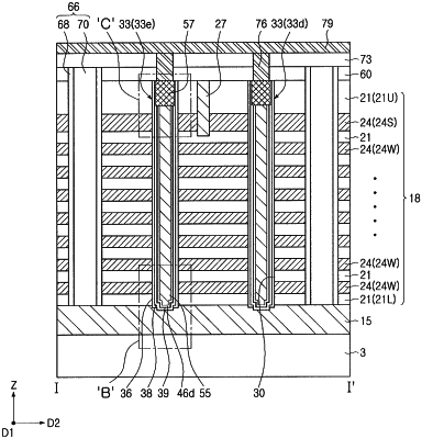
1. A semiconductor device, comprising:
a lower structure including an impurity region;
a stack structure on the lower structure;
separation structures penetrating the stack structure on the lower structure;
an opening penetrating the stack structure between the separation structures;
a vertical structure in the opening;
a contact plug electrically connected to the vertical structure on the stack structure; and
a bit line electrically connected to the contact plug on the contact plug,
wherein the stack structure includes interlayer insulating layers and gate electrodes in contact with each other and alternately layered,
wherein the vertical structure includes:
a core region having insulating properties and spaced apart from a side wall of the opening,
a semiconductor layer covering a side surface and a lower surface of the core region,
a gate dielectric layer between an external side surface of the semiconductor layer and the gate electrodes,
a data storage structure interposed between the core region and the semiconductor layer, and covering the side surface and the lower surface of the core region, and
a pad pattern in contact with an upper surface of the core region,
wherein an upper end of the data storage structure overlaps the pad pattern,
wherein the impurity region and the pad pattern include a doped silicon having N-type conductivity,
wherein the contact plug is in contact with the pad pattern, and
wherein the data storage structure includes a variable resistive material layer having an oxygen vacancy.
|