| CPC H10N 70/231 (2023.02) [H10B 63/80 (2023.02); H10N 70/8833 (2023.02)] | 21 Claims |
|
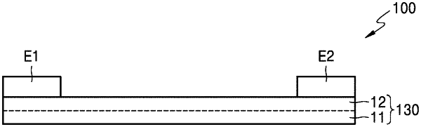
1. A variable resistance memory device comprising:
a variable resistance layer including a first layer, a second layer, and a third layer,
the second layer on the first layer,
the first layer including a first material,
the second layer including a second material having a valence different from a valence of the first material
the third layer on the second layer, the third layer including a third material having a valence different from a valence of the second material;
wherein each of the first layer, the second layer, and the third layer have a thickness of 10 nm or less; and
a first conductive element and a second conductive element on the variable resistance layer and separated from each other so that an electric current path is formed in the variable resistance layer in a direction perpendicular to a direction in which the first layer and the second layer are stacked.
|