| CPC H10N 50/10 (2023.02) [H10B 61/00 (2023.02); H10B 63/80 (2023.02); H10N 50/01 (2023.02); H10N 50/85 (2023.02); H10N 70/063 (2023.02); H10N 70/068 (2023.02); H10N 70/841 (2023.02); H10N 70/882 (2023.02)] | 20 Claims |
|
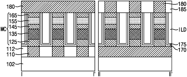
1. A method of manufacturing a variable resistance memory device, comprising:
forming a plurality of first conductive lines with an insulating pattern disposed between neighboring first conductive lines of the plurality of first conductive lines;
forming a stacked structure comprising a lower electrode layer, a variable resistance layer, and an upper electrode layer, which are sequentially stacked on the plurality of first conductive lines and the insulating pattern;
etching the stacked structure to form a plurality of memory cells, each comprising a lower electrode, a variable resistor, and an upper electrode;
forming an anti-oxidation layer covering the lower electrode, the variable resistor, and the upper electrode of the plurality of memory cells;
forming a capping layer covering the anti-oxidation layer; and
forming an interlayer insulating layer which fills a space between neighboring memory cells of the plurality of memory cells,
wherein the anti-oxidation layer includes SiCxHy.
|