| CPC H10N 50/10 (2023.02) [H01L 23/5283 (2013.01); H10B 61/22 (2023.02); H10N 50/01 (2023.02); H10N 50/80 (2023.02)] | 20 Claims |
|
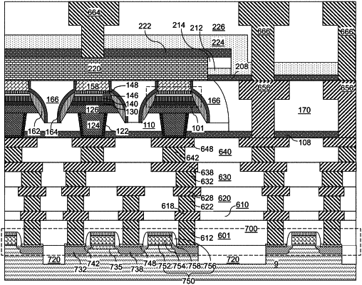
1. A memory array device, comprising:
an array of memory cells located over a substrate, wherein each of the memory cells comprises, from bottom to top, a bottom electrode, a memory element, and a top electrode;
a memory-level dielectric layer laterally surrounding the array of memory cells, wherein top surfaces of the top electrodes are located within a horizontal plane including a top surface of the memory-level dielectric layer;
top-interconnection metal lines laterally extending along a horizontal direction, wherein each of the top-interconnection metal lines contacts, or incorporates, a respective row of top electrodes;
an upper-level etch stop dielectric layer contacting a top surface of the memory-level dielectric layer and laterally surrounding the top-interconnection metal lines;
a dielectric matrix layer laterally surrounding the top-interconnection metal lines and having a top surface within a horizontal plane including top surface of the top-interconnection metal lines; and
a cap-level etch stop dielectric layer overlying the top-interconnection metal lines and having sidewalls that are vertically coincident with sidewalls of the dielectric matrix layer.
|