| CPC H10K 71/00 (2023.02) [H10K 50/844 (2023.02); H10K 59/124 (2023.02); H10K 59/40 (2023.02)] | 17 Claims |
|
1. A manufacturing method for a display substrate, wherein
the display substrate comprises a display area and a bonding area disposed at one side of the display area, wherein the bonding area comprises an isolation area disposed close to the display area and a bonding pad area disposed at one side of the isolation area away from the display area, and
the manufacturing method comprises:
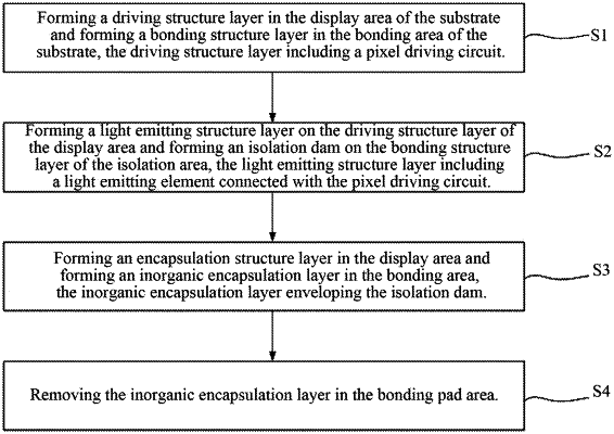
forming a driving structure layer in the display area of a substrate and forming a bonding structure layer in the bonding area of the substrate, wherein the driving structure layer comprises a pixel driving circuit,
forming a light emitting structure layer on the driving structure layer in the display area and forming an isolation dam on the bonding structure layer in the isolation area, wherein the light emitting structure layer comprises a light emitting element which is connected with the pixel driving circuit,
forming an encapsulation structure layer in the display area and forming an inorganic encapsulation layer in the bonding area, wherein the inorganic encapsulation layer envelops the isolation dam, and
removing the inorganic encapsulation layer in the bonding pad area,
wherein forming the encapsulation structure layer in the display area and forming the inorganic encapsulation layer in the bonding area comprises:
forming a first inorganic encapsulation layer on an entire surface of the substrate on which the light emitting structure layer and the isolation dam have been formed,
forming an organic encapsulation layer on the first inorganic encapsulation layer in the display area, and
forming a second inorganic encapsulation layer on the entire surface of the substrate on which the organic encapsulation layer has been formed.
|