| CPC H10K 59/65 (2023.02) [H10K 50/865 (2023.02); H10K 59/1213 (2023.02)] | 18 Claims |
|
1. A display device comprising:
a display panel including a substrate, wherein the display panel is divided into a first display region, in which a plurality of first pixels is disposed, and a second display region, in which a plurality of second pixels is disposed; and
a sensor overlapping the second display region of the display panel,
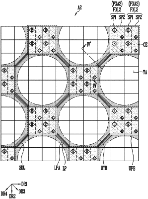
wherein the second display region includes a plurality of unit pixel blocks, each including two by two second pixels adjacent to each other in a first direction and in a second direction intersecting the first direction, and a transmissive region through which light is transmitted,
wherein, in a plan view, a distance between two unit pixel blocks adjacent to each other in the first direction is greater than a distance between two unit pixel blocks adjacent to each other in an oblique direction inclined to the first direction, and
wherein, in at least one region of the second display region, which are surrounded between the unit pixel blocks, a ratio of areas occupied by a region of the second pixels and the transmissive region is about 2:9,
wherein the display panel further comprises:
a line part disposed between the unit pixel blocks; and
a light blocking pattern disposed on the substrate in at least one region of the second display region,
wherein the light blocking pattern overlaps the line part,
wherein the transmissive region includes a plurality of unit transmissive blocks, each having substantially a circular shape,
wherein each of the first and second pixels comprises a first electrode, an emitting layer disposed on the first electrode, and a second electrode disposed on the emitting layer, and
wherein the second electrode is not disposed in the unit transmissive blocks.
|