| CPC H10K 59/40 (2023.02) [G06F 3/044 (2013.01); G06F 3/0412 (2013.01); H10K 50/86 (2023.02); H10K 50/865 (2023.02); H10K 59/122 (2023.02)] | 15 Claims |
|
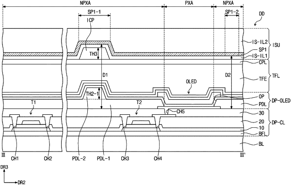
1. A display device comprising:
a display panel; and
an input sensing unit comprising a sensing electrode and disposed directly on the display panel,
wherein:
the display panel comprises:
a light emitting element comprising a first electrode, which contacts a base insulation layer, a second electrode, and a light emitting layer disposed between the first electrode and the second electrode;
a pixel defining layer disposed below the second electrode, contacting the base insulation layer, and comprising a first portion, in which an opening to expose the first electrode is defined, and a second portion, which is disposed on the first portion and overlaps the first portion;
a plurality of thin-films disposed on the second electrode; and
an insulation pattern disposed on the plurality of thin-films, overlapping the pixel defining layer, and overlapping the second portion; and
a shortest distance between a first portion, which overlaps the insulation pattern, of the sensing electrode and the base insulation layer in a thickness direction of the display device is greater than a shortest distance between a second portion, which non-overlaps the insulation pattern, of the sensing electrode and the base insulation layer in the thickness direction of the display device.
|