| CPC H10K 59/40 (2023.02) [G06F 3/0412 (2013.01); H04B 1/3888 (2013.01); H04M 1/0266 (2013.01); H10K 50/11 (2023.02); H10K 50/84 (2023.02); H10K 50/841 (2023.02); H10K 50/844 (2023.02); H10K 59/131 (2023.02); H10K 71/80 (2023.02); H10K 77/111 (2023.02); G06F 2203/04103 (2013.01); G09G 2380/02 (2013.01); H01L 27/14678 (2013.01); H10K 59/1201 (2023.02); H10K 59/126 (2023.02); H10K 59/60 (2023.02); H10K 2102/311 (2023.02); Y02E 10/549 (2013.01)] | 10 Claims |
|
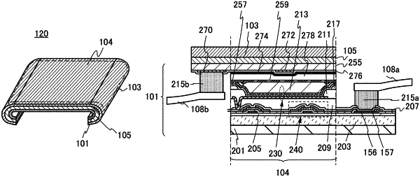
1. A light-emitting device comprising:
a transistor over a first substrate;
a light-emitting element over the transistor;
a first conductive layer over the light-emitting element;
an insulating layer over the first conductive layer;
a second conductive layer over the insulating layer; and
a second substrate over the second conductive layer,
wherein a third conductive layer is of a same material as the second conductive layer,
wherein the third conductive layer is electrically connected to a flexible printed circuit,
wherein the third conductive layer is configured as an external connection electrode,
wherein the transistor and the light-emitting element are in a pixel region,
wherein the first conductive layer and the second conductive layer overlap with each other in the pixel region with the insulating layer therebetween,
wherein the third conductive layer is outside the pixel region,
wherein the second substrate comprises a flat region and a first region which is bent to the first substrate side,
wherein the pixel region and the first region overlap with each other,
wherein the third conductive layer and the flat region overlap with each other, and
wherein the light-emitting device is configured to sense proximity or contact of an object on a top surface of the second substrate using the first conductive layer and the second conductive layer.
|