| CPC H10K 59/352 (2023.02) [H10K 50/818 (2023.02); H10K 50/84 (2023.02); H10K 59/122 (2023.02); H10K 59/40 (2023.02)] | 18 Claims |
|
1. A display panel including a plurality of sub-pixels, comprising:
a substrate;
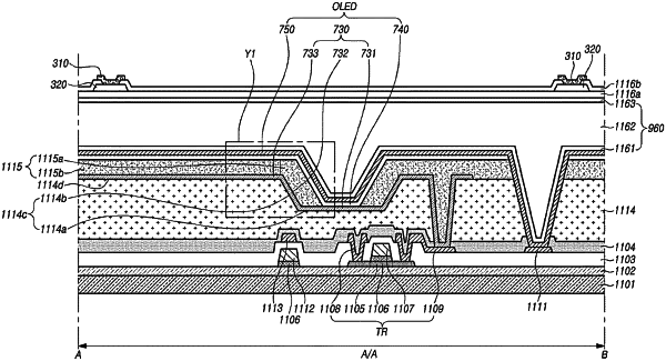
an insulating film on the substrate and including a concave portion having a flat portion and an inclined portion surrounding the flat portion in one or more of the plurality of sub-pixels;
a first electrode on the insulating film, on an upper portion of the concave portion, and on a periphery portion extending from the concave portion, in the one or more sub-pixels;
a bank on the first electrode and the insulating film, and having an opening corresponding to a part of the flat portion in the one or more sub-pixels;
a light emitting layer on the first electrode and in the opening of the bank in the one or more sub-pixels;
a second electrode on the light emitting layer and the bank;
an encapsulation layer on the second electrode; and
a plurality of touch electrodes disposed on the encapsulation layer, each one of the plurality of touch electrodes including an open area,
wherein, in a viewing plane, the open area of at least one of the sub-pixels includes a first area through which light from the light emitting layer exits, a non-emission area completely surrounding the first area, and a second area around the non-emission area through which light from the light emitting layer exits.
|