| CPC H10K 59/131 (2023.02) [H10K 59/121 (2023.02); H10K 59/122 (2023.02); H10K 59/88 (2023.02); H10K 59/35 (2023.02)] | 23 Claims |
|
1. A display apparatus comprising:
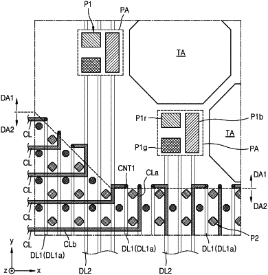
a substrate comprising a first area having a transmission portion, and a second area surrounding the first area;
a first data line extending in a first direction on the second area, and comprising a first line and a second line spaced from each other with the first area therebetween;
a connection line on the second area, adjacent to, and bypassing, the first area, and comprising an end connected to the first line, and another end connected to the second line;
a pixel circuit on the second area, comprising a thin-film transistor, and a node connection line electrically connected to the thin-film transistor; and
a first pixel electrode above the pixel circuit,
wherein the connection line is spaced from the node connection line.
|