| CPC H10K 59/131 (2023.02) [G09G 3/3233 (2013.01); G09G 2300/0842 (2013.01); G09G 2310/0202 (2013.01)] | 14 Claims |
|
1. A display device, comprising:
a plurality of data lines to supply data signals;
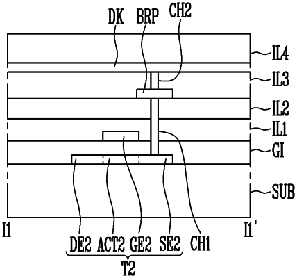
a plurality of pixels each comprising a light-emitting element, a first transistor to control current flowing through the light-emitting element, a second transistor connected between the first transistor and one of the plurality of data lines, a third transistor connected between a second electrode and a gate electrode of the first transistor, a fourth transistor connected between a first electrode of the third transistor and an initialization power source, and an initialization transistor connected between the initialization power source and a first electrode of the light-emitting element, each of the first transistor, the second transistor, the third transistor, the fourth transistor and the initialization transistor comprising a semiconductor pattern; and
a conductive pattern disposed on and connected to the second transistor through a first contact hole,
wherein the data line is disposed on a layer different from that of the conductive pattern, and is connected to the conductive pattern through a second contact hole,
wherein the first contact hole and the second contact hole overlap each other, when viewed on a plane,
wherein the data line and the conductive pattern overlap the semiconductor pattern of the second transistor without overlapping the semiconductor pattern of each of the fourth transistor and the initialization transistor,
wherein each of the plurality of data lines comprises a first sub data line extending in a first direction and a second sub data line extending in the first direction,
wherein the first sub data line and the second sub data line are provided on both sides of a pixel column in which at least two or more of the plurality of pixels are arranged in the first direction,
wherein one of the pixels of the pixel column is connected to the first sub data line, and another one of the pixels of the pixel column adjacent to the one of the pixels connected to the first sub data line is connected to the second sub data line,
wherein each of the pixels of the pixel column is connected to one of the first sub data line and the second sub data line, and
wherein an active pattern of the second transistor does not overlap the conductive pattern.
|