| CPC H10K 59/131 (2023.02) [H10K 59/122 (2023.02); H10K 59/1201 (2023.02)] | 11 Claims |
|
1. A display device comprising:
a substrate comprising a first region in which a first pixel circuit is located, and a second region in which a second pixel circuit is located;
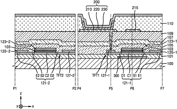
a first active layer located on the first region, and comprising a first channel region, a first source region at a first side of the first channel region, a first drain region at a second side of the first channel region, and a first extension region extending in a direction from the first source region to the second region;
a first gate electrode located above the first active layer, and overlapping the first channel region;
a gate insulating layer between the first active layer and the first gate electrode in a region overlapping the first gate electrode;
a driving voltage line located directly on the first active layer, overlapping the first source region, in a same layer as the gate insulating layer, and extending along the first extension region;
a first connection electrode located on the first drain region; and
a pixel electrode located above the first gate electrode and connected to the first connection electrode.
|
|
11. A display device comprising:
a substrate comprising a first region in which a first pixel circuit is located, and a second region in which a second pixel circuit is located;
a first active layer located on the first region, and comprising a first channel region, a first source region at a first side of the first channel region, a first drain region at a second side of the first channel region, and a first extension region extending in a direction from the first source region to the second region;
a first gate electrode located above the first active layer, and overlapping the first channel region;
a driving voltage line located on the first active layer, overlapping the first source region, and extending along the first extension region;
a first connection electrode located on the first drain region;
a pixel electrode located above the first gate electrode and connected to the first connection electrode;
a second active layer located on the first region, and comprising a second channel region, a second source region at a first side of the second channel region, a second drain region at a second side of the second channel region, and a second extension region extending in a direction from the second source region to the first region;
a second gate electrode located above the second active layer, and overlapping the second channel region;
a data line located on the second active layer, overlapping the second source region, and extending along the second extension region;
a second connection electrode located on the second drain region; and
a bridge electrode electrically connecting the second connection electrode to the first gate electrode, and comprising a same material as the pixel electrode, and has a layered structure that is the same as a layered structure of the pixel electrode.
|