| CPC H10K 59/131 (2023.02) [H01L 28/60 (2013.01); H10K 59/123 (2023.02); H10K 59/1216 (2023.02); H10K 59/35 (2023.02)] | 13 Claims |

|
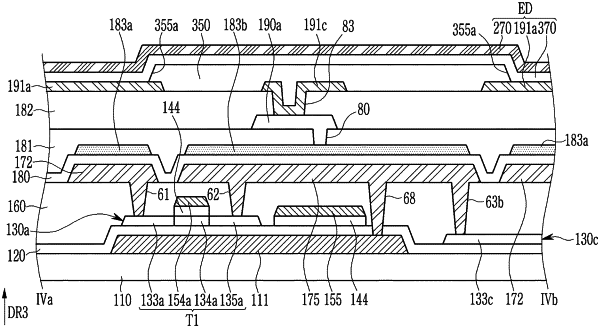
1. A display device comprising:
a first pixel circuit portion including at least one transistor;
a second pixel circuit portion including at least one transistor;
a first pixel electrode electrically connected to the first pixel circuit portion;
a second pixel electrode electrically connected to the second pixel circuit portion;
a first data line electrically connected to the first pixel circuit portion; and
a second data line electrically connected to the second pixel circuit portion,
wherein the first data line and the second data line are arranged adjacent to each other along a first direction,
wherein the second pixel circuit portion overlaps the first data line and the second data line in a plan view, and
wherein the first pixel circuit portion and the second pixel circuit portion are arranged along a second direction perpendicular to the first direction.
|