| CPC H10K 59/126 (2023.02) [H10K 50/11 (2023.02); H10K 50/822 (2023.02); H10K 71/621 (2023.02)] | 23 Claims |
|
1. A display panel comprising:
a first display area comprising a plurality of first light emitting areas;
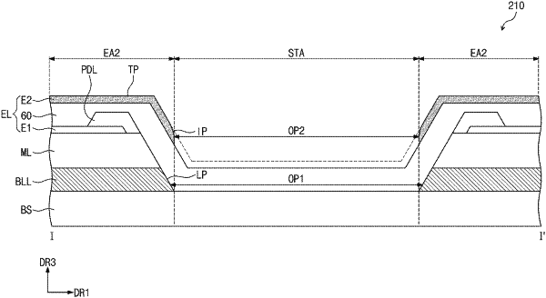
a second display area adjacent to the first display area in a plan view of the display panel and comprising a plurality of second light emitting areas and a signal transmission area adjacent to the plurality of second light emitting areas in the plan view of the display panel, wherein the plurality of second light emitting areas in the second display area has a first transmittance, and the signal transmission area in the second display area has a second transmittance that is higher than the first transmittance of the plurality of second light emitting areas;
a base substrate;
a circuit element layer disposed on the base substrate;
a light blocking pattern disposed between the base substrate and the circuit element layer, overlapping the plurality of first light emitting areas and the plurality of second light emitting areas, and having a first opening corresponding to the signal transmission area; and
a light emitting element layer disposed on the circuit element layer and comprising:
a first electrode overlapping the plurality of first light emitting areas and the plurality of second light emitting areas;
a light emitting layer disposed on the first electrode and corresponding to at least the plurality of second light emitting areas; and
a second electrode overlapping the plurality of first light emitting areas and the plurality of second light emitting areas.
|